
In our previous post, we provided an overview of the STM32 family and outlined the selection criteria for flight controller applications. In this article, we will dig deeper into the internal architecture of the STM32H7 series—the current modern standard for industrial FCs—and break down the specific differences between the H743, H745, H753, and H7A3 to help you determine the optimal choice for your specific design requirements.
Shared Architecture of the H7 Series
The STM32H7 series microcontrollers are all built around the high-performance ARM Cortex-M7 core and share several architectural advantages:
- Superscalar Execution Engine: Features a 6-stage superscalar pipeline, branch prediction, and a Harvard architecture L1 cache (16 KB Instruction + 16 KB Data). Equipped with a double-precision hardware Floating Point Unit (FPU) and advanced DSP extension instructions, it accelerates heavy matrix math operations like those found in the EKF. This optimized caching and pipelining allow the H7 to deliver vastly superior real-world performance over the F4/F7 series, even at identical clock frequencies.
- Tightly Coupled Memory (TCM): A critical differentiator for flight control dynamics. TCM is wired directly to the CPU core, ensuring zero-wait-state access regardless of cache hits or misses. By separating ITCM (Instruction TCM, 64 KB) and DTCM (Data TCM, 128 KB), developers can isolate time-critical interrupt handlers and main control loop code to ITCM, guaranteeing strict deterministic execution times.
- AXI/AHB Bus Matrix: Connects the CPU, DMA controllers, and high-speed peripherals via an unmanaged, high-bandwidth parallel bus structure. This architecture is perfect for FC design, enabling high-rate IMU data DMA streaming to execute concurrently with heavy flight stabilization mathematics without stalling the bus.
STM32H743: The Definitive First Choice
The STM32H743 is currently the leading candidate for custom industrial flight controller developments.
Specification PillarDetails and Architectural AdvantagesCore ArchitectureSingle-core Cortex-M7 operating up to 480 MHz. Equipped with 2 MB Flash (dual-bank configurable), 1 MB contiguous RAM, 64 KB ITCM, and 128 KB DTCM.Peripheral DensityFeatures a highly integrated pinout optimized for aerospace telemetry: 6x SPI, 4x I2C, 8x UART/USART, 2x FDCAN, 2x USB OTG (FS+HS), 2x SAI, 2x SDMMC, and 3x 16-bit ADCs along with a generous complement of timers.Common PackagesH743VIT6 (100-pin LQFP) and H743IIT6 (176-pin LQFP). The H743VIT is the exact variant running inside the industry-standard Cube Orange+, ensuring unmatched ArduPilot software maturity. Its pin count fits standard medium industrial multirotors perfectly. The H743IIT offers more I/O expandability for complex enterprise platforms.Memory HeadroomThe 2 MB dual-bank Flash easily accommodates ArduPilot's compiled binary footprint (~1 MB) and bootloaders while leaving plenty of room for look-up tables. Dual-bank functionality permits robust Over-The-Air (OTA) firmware updates, maintaining execution on one bank while flashing the other.
Development Hint: The ArduPilot source tree houses an absolute goldmine of reference targets natively tracking the H743 (e.g., CubeOrange, KakuteH7, MatekH743). Referencing these configuration matrices saves significant development time during custom pinout definitions.
STM32H745 / STM32H755: Dual-Core Potential vs. Reality
The H745 and H755 represent the asymmetric dual-core evolution of the H743/H753 family, stacking a Cortex-M7 (up to 480 MHz) and a Cortex-M4 (up to 240 MHz) onto a single silicon die.
The theoretical advantage is clear: you can offload the primary flight stack overhead (EKF state estimation, 3D position navigation, mission orchestration) to the M7 core while isolating the critical inner attitude stabilization loop and high-rate ESC communication onto the M4 core. This prevents any high-level processing spikes on the M7 from degrading real-time attitude loop stability.
However, the practical barriers are significant:
Open-source flight stacks like ArduPilot do not natively support dual-core execution layouts out of the box. Running ArduPilot on an H745 defaults the chip to a single-core mode, utilizing only the M7 core. Exploiting the M4 core requires implementing custom inter-core communication channels (via hardware semaphores [HSEM] and shared memory buffers) and writing bespoke low-level firmware for the M4 side yourself.
Managing the resulting inter-core communication latency and data consistency is complex and inflates software development overhead. Consequently, choosing the H745 only makes sense if you plan to forego open-source stacks in favor of a completely custom bare-metal architecture, or if you want to future-proof your hardware layout for eventual dual-core software migration.
(Note: The H755 adds hardware cryptographic engines—including PKA, HASH, RNG, and AES—to the dual-core design, making it suitable for secure, mission-critical defense frameworks).
STM32H753: When Security is Mandatory
The STM32H753 is an upgraded, security-focused version of the H743. It incorporates a dedicated hardware cryptographic acceleration engine (supporting AES-256, SHA, and Public Key Acceleration [PKA]), a true hardware Random Number Generator (RNG), and ARM TrustZone integration.
The choice to deploy an H753 over an H743 is driven entirely by external requirements rather than flight dynamics:
- Government or defense-sector strict secure-boot requirements.
- End-to-end encrypted MAVLink telemetry streaming over the air.
- Secure cryptographic signature storage for compliance with Remote ID regulations.
From a raw processing and flight performance perspective, the H753 is identical to the H743, with a negligible increase in current draw when the crypto engine is active. If your project lacks specific security compliance mandates, the H743 remains more cost-effective.
STM32H7A3 / STM32H7B3: High Performance Meets Lower Power
Released after the initial H7 series, the H7A3 and H7B3 represent a newer architectural generation targeting a different power envelope.
- Power Efficiency: While the maximum core clock is lower than the H743 (280 MHz vs. 480 MHz), these chips utilize a lower-leakage manufacturing process (40nm LP). This significantly reduces operational current draw. For long-endurance, battery-constrained UAV platforms, this power savings directly extends flight time.
- Modified Memory Architecture: The H7A3 bumps internal RAM up to a generous 1.4 MB paired with 2 MB Flash. The H7B3 is a flashless variant designed around external memory architectures. While a flashless design opens up PCB placement flexibility, it requires a careful high-speed layout to route external SPI or OctoSPI (OSPI) Flash lines without signal corruption.
ArduPilot includes several H7A3 targets, but the hardware track record is less dense than the H743 branch. If your mission profile requires keeping power consumption minimal over long flights or running large software allocations requiring more RAM, the H7A3 is an attractive choice.
How to Decode STM32 Part Number Suffixes
Understanding STMicroelectronics' naming convention allows you to quickly identify key hardware specifications straight from a part number without opening a datasheet:
[Image breaking down the alphanumeric code of STM32H743VIT6 into Family, Series, Sub-line, Pin Count, Flash Size, Package, and Temperature Grade]
Taking the STM32H743VIT6 as an example:
- STM32: Family name.
- H7: Series designation (H = High Performance).
- 43: Sub-line architecture (43 = Single-core, standard security).
- V: Pin count variant (V = 100 pins, Z = 144 pins, I = 176 pins, N = 216 pins).
- I: Internal Flash capacity (G = 1 MB, I = 2 MB).
- T: Package type (T = LQFP, H = TFBGA, U = UFQFPN).
- 6: Industrial temperature operation window (6 = -40°C to 85°C).
For flight controllers, package selection is crucial. The V (100-pin LQFP) package is highly favored in medium-scale commercial FCs because it balances easy assembly and PCB routing with plenty of I/O. The I (176-pin LQFP) package is preferred for enterprise platforms with extensive peripheral suites. BGA packages (like the 216-pin N variant) are typically avoided for small-scale production runs due to the high assembly and X-ray inspection complexity they introduce.
Step-by-Step MCU Selection Flow
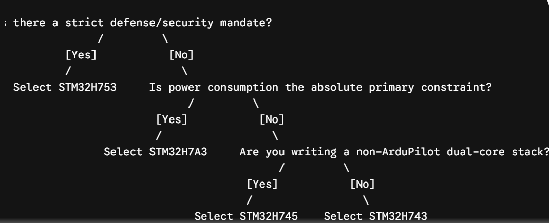
- Evaluate Software & Security Baseline: If you are building a standard industrial platform around ArduPilot/PX4, your default baseline is the H743. If you have custom regulatory cryptographic requirements, step up to the H753.
- Review I/O Requirements: Map your entire sensor suite (number of SPI IMUs, I2C buses, GPS UARTs, and CAN links). If everything routes cleanly within 100 pins, select the H743VIT6. If your routing density breaks the 100-pin limit, scale up to the H743IIT6.
Engineering Caveats When Running ArduPilot on the H7
Developing custom hardware around the H7 family introduces several unique software-hardware behaviors that require careful management:
- RAM Bank Allocation & Split Domains: The H7's 1 MB RAM is not a single contiguous block; it is segmented into distinct memory domains (AXI SRAM, SRAM1-4, Backup SRAM, and TCM). Each domain communicates over different bus matrices at different speeds. If your custom hwdef.dat or linker scripts map high-rate stacks, heaps, or DMA ring-buffers into mismatched RAM blocks, you will experience severe performance drops or outright DMA faults.
- DMA and Cache Coherency: Because the H7 utilizes a high-speed L1 cache, data modified by the CPU might sit in the cache and not be immediately committed to physical RAM. If a DMA operation then pushes data from a peripheral (like an SPI IMU) directly into RAM, the CPU may continue reading the stale cached data instead. While ArduPilot's core HAL manages this cache invalidation automatically for standard configurations, writing custom device drivers requires explicit cache-management handling.
- Clock Tree Configurations (Independent PLLs): The H7 features complex clock tree distribution boards where PLL1 clocks the main CPU core and AHB buses, PLL2 clocks standard communication peripherals (SPI, I2C), and PLL3 drives specialized blocks like USB and SDMMC. Your maximum achievable SPI clocking depends entirely on how you balance your PLL2 multipliers; ensuring your high-speed IMUs can communicate at their full rated speed (such as 24 MHz for the ICM-42688-P) requires reviewing these clock distributions.
Summary
Selecting an MCU from the STM32H7 series can be aligned with four main application pathways: the H743 for standard industrial FC platforms, the H753 for cryptographic and defense compliance, the H745 for highly customized dual-core developments, and the H7A3 for low-power, long-endurance platforms. For the vast majority of custom commercial flight control projects, the STM32H743VIT6 remains the safest and most reliable starting point.
In our next installment, FC5, we will move from chip architectures to software integration, detailing the internal file structure of ArduPilot's hwdef.dat and defining the minimum required hardware configurations to bring up a custom board.